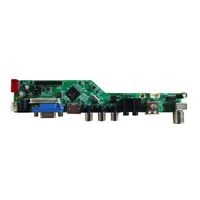
6/8 bit FHD LCD panel VGA AV connector LCD control board")
LVDS signal 1920x1080(UFG) 6/8 bit FHD LCD panel VGA AV connector LCD control board
- $6.00 /set
- 1 set
- Shenzhen Caison Technology Co., Ltd.
- Guangdong, China
- Mr Alex chao
| port: | Hongkong | brand: | Kayson |
| Supply capacity: | 999 acres per month | payment terms: | L/C,Western Union,T/T |
| Display size: | 8.8-86 inches | Packaging Details: | Bubble bag + carton |
| Packaging Preview: | place of origin; place of origin: | Guangdong, China | |
| type: | TFT | model: | Thermal resistance 2660 |
LVDS Signal 1920x1080(UFG) 6/8 Bit FHD LCD Panel VGA AV Connector LCD Controller Board
1. General Instructions
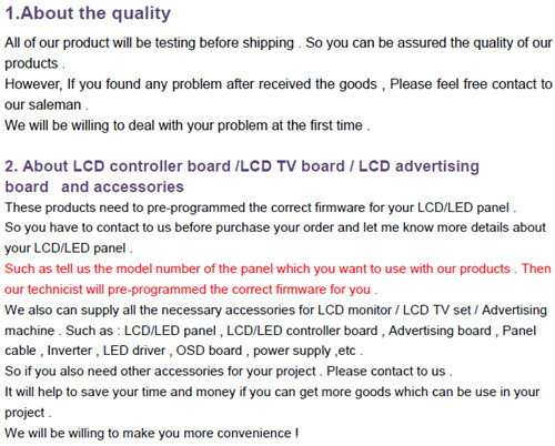
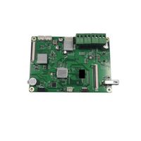
RTD2662 V2.0 is a multifunctional LCD control board that supports +VGA+AV video signal input and 50Pin TTL+30P LVDS signal output. The maximum output resolution can reach 1920X1080 (1080P).
RTD2662 V2.0 can provide 3.3V power supply for LCD panel. So it is designed for 7~18.1” LCD panel.
2. Features
|
chipset |
Thermal resistance 2662 |
|
|
Support LCD panel |
interface |
Dual LVDS |
|
Resolution |
Up to 1920X1080@60Hz |
|
|
strength |
Board Requirements |
5~24V DC power supply |
|
to LCD panel |
3.3V |
|
|
manage |
low power mode |
|
|
Stanby |
>2W |
|
|
On-screen language |
Simplified Chinese, Traditional Chinese, English, French, German, Italian, Spanish, Russia, Japan, Korea |
|
|
Key Function |
Power, Menu, Up, Down, Source |
|
|
video input |
1+1 VGA+2 AV |
|
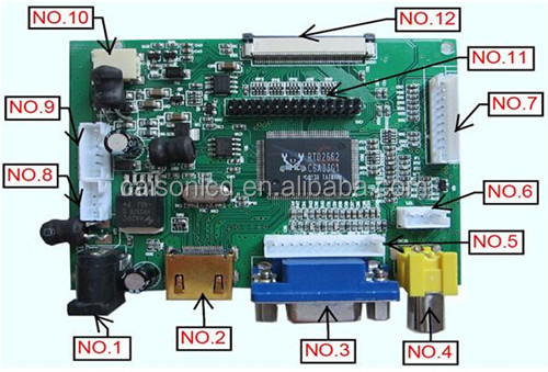
3. Functional layout
The picture is for reference only, the actual product is the standard.
RTD2660 V2.0 Top View
|
Do not |
describe |
Do not |
describe |
|
1 |
power input |
7 |
Keyboard & IR & LED Indicators |
|
2 |
signal input |
8 |
power input |
|
3 |
VGA signal input |
9 |
Power and control signals for additional inverter boards |
|
4 |
AV1 signal input |
10 |
Backlight Voltage Output Connector |
|
5 |
Additional VGA signal input |
11 |
LVDS signal output connector |
|
6 |
Additional AV1 and AV2 signal inputs |
12 |
TTL signal output connector |
4. Interface definition:
LVDS signal output interface:
|
Needle size |
definition |
describe |
|
1 |
VCC |
LCD/LED panel power supply |
|
2 |
VCC |
|
|
3 |
VCC |
|
|
4 |
ground |
ground |
|
5 |
ground |
|
|
6 |
ground |
|
|
7 |
RXOC- |
Negative LVDS channel O0 (odd) |
|
8 |
RXOC+ |
Positive LVDS channel O0 (odd) |
|
9 |
RXO0- |
Negative LVDS channel O1 (odd) |
|
10 |
RXO0+ |
Positive LVDS channel O1 (odd) |
|
11 |
RXO1- |
Negative LVDS channel O2 (odd) |
|
12 |
RXO1+ |
Positive LVDS channel O2 (odd) |
|
13 |
ground |
ground |
|
14 |
ground |
ground |
|
15 |
RXOC- |
Negative sample clock (odd) |
|
16 |
RXOC+ |
Positive sample clock (odd) |
|
17 |
RXO3- |
Negative LVDS channel O3 (odd) |
|
18 |
RXO3+ |
Positive LVDS channel O3 (odd) |
|
19 |
RXE0- |
Negative LVDS channel E0 (even) |
|
20 |
RXE0+ |
Positive LVDS channel E0 (even) |
|
twenty one |
RXE1- |
Negative LVDS channel E1 (even) |
|
twenty two |
RXE1+ |
Positive LVDS channel E1 (even) |
|
twenty three |
RXE2- |
Negative LVDS channel E2 (even) |
|
twenty four |
RXE2+ |
Positive LVDS channel E2 (even) |
|
25 |
ground |
ground |
|
26 |
ground |
ground |
|
27 |
RXEC- |
Negative sample clock (even) |
|
28 |
Receive EC+ |
Positive sample clock (even) |
|
29 |
RXE3- |
Negative LVDS channel E3 (even) |
|
30 |
RXE3+ |
Positive LVDS channel E3 (even) |
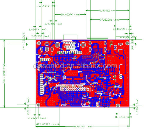
5.PCB mechanical dimensions:
1. About packaging
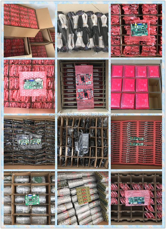
2. About shipping costs