Multilayer pcb circuit board manufacturer 1~30 layers
- $0.20 / 10 - 999 pieces
$0.15 / >=1000 pieces - 10 pieces
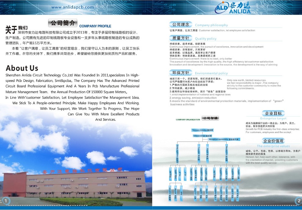
- Shenzhen Anlida Electronics Technology Co., Ltd.
- Guangdong, China
- Mr Ken Zhang
PRODUCT DETAIL
| payment terms: | L/C, Western Union, D/P, D/A, T/T, MoneyGram, Paypal | product name: | ru 94VO printed circuit board |
| Applications: | 94VO circuit board | Board Dimensions: | green/regular/red/black/yellow |
| Impedance Control: | 50/90/100±10% ohm | place of origin; place of origin: | Guangdong, China |
| product design: | Anlida Design | TG value: | T150-180 |
| Shenzhen circuit board: | One-stop service | port: | Shenzhen, China (Mainland) |
| Minute line width: | 0.05mm/2mil | brand: | Anli Dapu circuit board |
| Flame retardant: | 94v0 | Plate thickness: | 0.15-10mm |
| Packaging Details: | Blister and carton and email: PCB design file, manufacturing file, DXF file, PAST file, Silk file, XY coordinate file. | model: | M10-Y |
| Minute Hole Size: | 0.1mm/4mil | standard: | IPC-A-610G CLASS II&III |
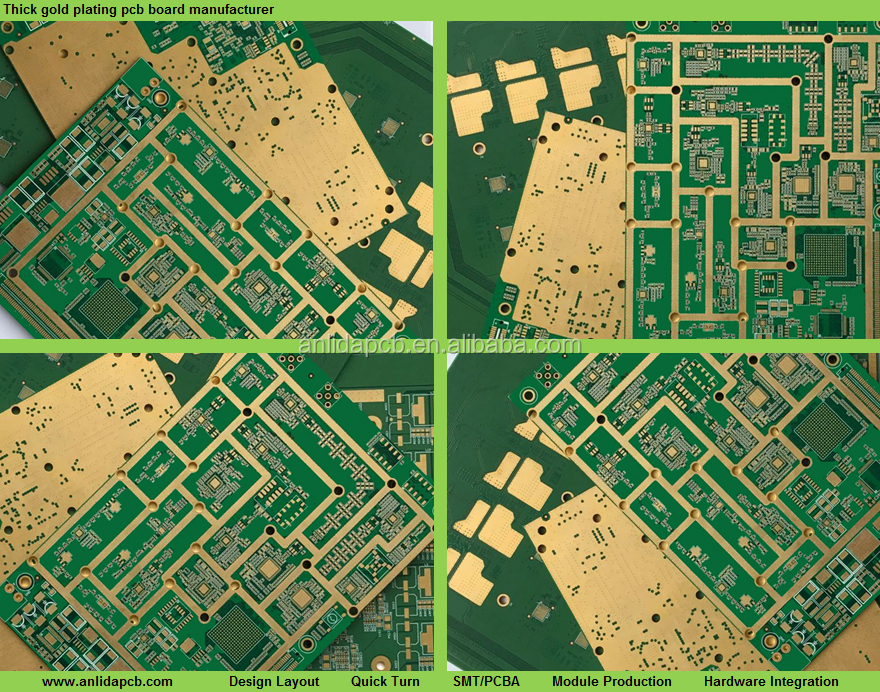
| Surface treatment: | ENIG OSP Sandblasting | Supply capacity: | 80000 square meters / month thick gold plating |
| Layers: | 1-40 floors, 12 floors | Minute line spacing: | 0.06 mm/2.5 million |
| Substrate: | FR-4/PI/FR-4 High TG | Package preview: | |
| Copper thickness: | 0.25 oz - 12 oz | Main services: | design manufacture assembly |
| type: | multilayer board |
Product Description
1~30 Layers Multilayer pcb circuit board manufacturer
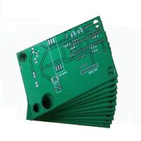
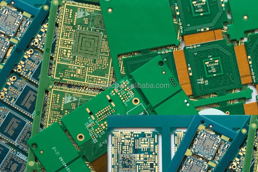
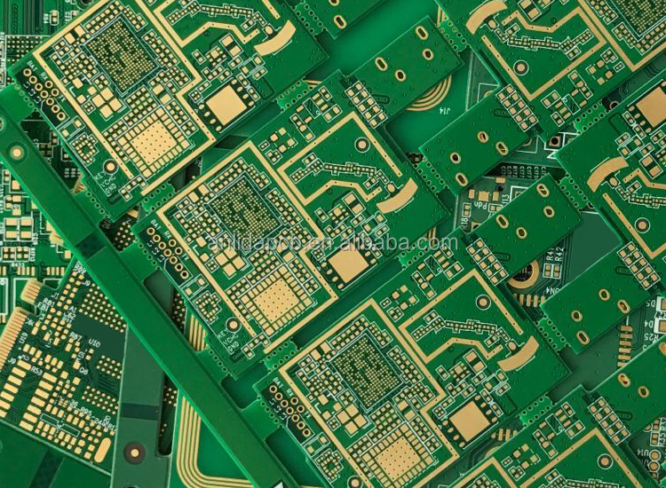
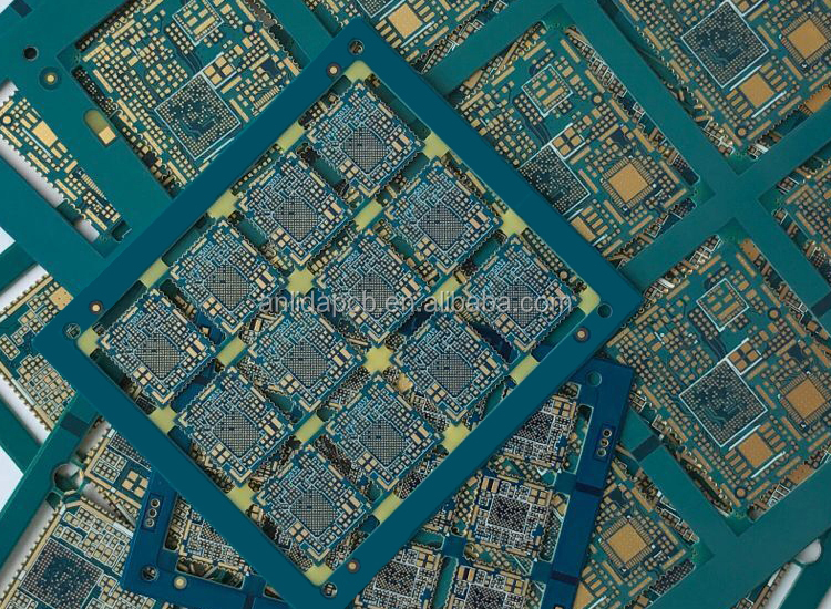
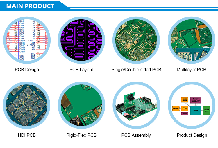
PCB product display:
All services:
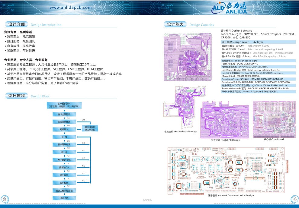
- High speed PCB design/PCB layout
- High speed PCB SI/PI/EMC analysis
- PCB reverse engineering design, engineering and early design support
- PCBA reverse engineering design
- Rapid 1-24LPCB prototyping, small to medium batch manufacturing
- Professional HDI PCB production
- Rigid-flex board manufacturing
- SMT assembly/PCBA assembly
- PCB parts procurement
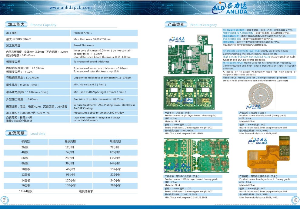
PCB parameters:
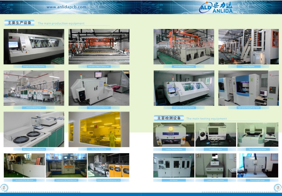
Printed circuit board production:
| Do not. | thing | prototype | mass production |
| 1 | layers | 1-30 floors | 1-20 floors |
| 2 | Maximum panel size | ≤1000X1000mm | ≤700X700mm |
| 3 | Substrate type | FR4, High Tg FR4, Rogers, Halogen Free | FR4, High Tg FR4, Rogers, Halogen Free |
| 4 | Maximum plate thickness | ≤10 mm | ≤10mm |
| 5 | Minimum plate thickness | 2L≥0.2mm, 4L≥0.3mm 6L≥0.4mm, 8L≥0.6mm 10L≥0.65mm, 12L≥0.8mm |
2L≥0.2mm, 4L≥0.3mm 6L≥0.4mm, 8L≥0.6mm 10L≥0.65mm, 12L≥0.8mm |
| 6 | Minimum Line Width | ≥ 0.05mm(2mil) | ≥ 0.064mm (2.5 million) |
| 7 | Minimum line spacing | ≥ 0.064mm (2.5 million) | ≥0.075mm (3 million) |
| 8 | Minimum via | 0.15 mm (6 million) | 0.15 mm (6 million) |
| 9 | Minimum blind hole | 0.1 mm (4 million) | 0.1 mm (4 million) |
| 10 | Minimum Buried Via | 0.2mm (8 million) | 0.2mm (8 million) |
| 11 | Minimum Plated Hole Thickness | 20µm (0.8 million) | 20µm (0.8 million) |
| 12 | surface coating | HASL, ENIG, OSP, ENIG+OSP, electroplating Ni/Au/Ag | HASL, ENIG, OSP, ENIG+OSP, electroplating Ni/Au/Ag |
| 13 | Solder mask color | Green, blue, black, white, yellow, red | Green, blue, black, white, yellow, red |
| 14 | Screen printing color | white, black, yellow, red, | white, black, yellow, red, |
| 15 | thick copper | 6oz/210µm | 4oz/140µm |
| 16 | Minimum S/M spacing | 0.1 mm (4 million) | 0.1 mm (4 million) |
| 17 | PTH diameter tolerance | ±0.076mm(±3mil) | ±0.076mm(±3mil) |
| 18 | NPTH Diameter Tolerance | ±0.05mm(±2mil) | ±0.05mm(±2mil) |
| 19 | Hole position deviation | ±0.05mm(±2mil) | ±0.05mm(±2mil) |
| 20 | Profile Tolerance | ±0.15mm (±6mil) | ±0.15mm (±6mil) |
| twenty one | Controllable Impedance | +/-5% | +/-10% |
| twenty two | twist and twist | ≤0.75% | ≤0.75% |
| twenty three | Flammability rating | 94V-0 | 94V-0 |
| twenty four | Solderability Test | 255℃+/-5℃ | 255℃+/-5℃ |
| 25 | Thermal Stress | 288+5℃, 10 seconds | 288+5℃, 10 seconds |
| 26 | Test voltage | 50-330V | 50-330V |
| 27 | Adhesion test | no peeling | no peeling |
| 28 | Other inspection items | IPC-6012/A-600H | IPC-6012/A-600H |
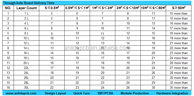
Production lead time:

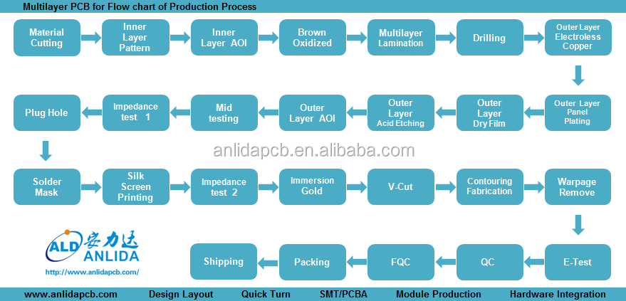
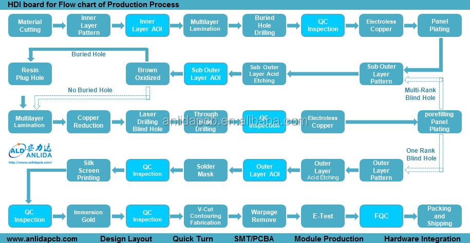
flow chart:
main products
VIEW MORE