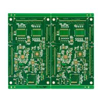
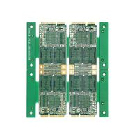
Pcb Hdi High Speed Prototyping Pcb Printed Circuit Board Layout
- $1.00 /piece
- 1 piece
- Shenzhen Jingbang Electronics Co., Ltd.
- Guangdong, China
- Mr Jeff Su
| minute. Line spacing: | 0.075mm | Surface treatment: | HASL, ENIG, Immersion Silver, Immersion Tin, OSP |
| Solder Mask Color: | Green, white, black, red, blue... | Certificate: | IATF16949, ISO13485, ISO9001, ISO14001 |
| Maximum size of veneer: | 700*460mm | model: | PCB and SMT assembly |
| Packaging Details: | Packaging Details: High Quality Shockproof Package Inner: Blister + Cardboard Outer: Carton | Substrate: | FR4, High TG FR4, High Frequency, Alum, FPC |
| place of origin; place of origin: | Guangdong, China | Silkscreen Color: | white, black, yellow, blue... |
| Minimum Solder Mask Clearance: | 0.07mm | brand: | Fast PCBA |
| PCB outline: | Square, round, irregular (with clamp) | port: | Shenzhen/Hong Kong |
| payment terms: | L/C,Western Union,D/P,D/A,T/T,MoneyGram | Copper Thickness: | 0.5-4 0z |
| Serve: | One-stop PCBA service | Layers: | 1-48 |
| Supply capacity: | 10000 pieces per week | minute. Line width: | 0.075mm |
| Subassembly: | plastic, metal, screen | Minimum order quantity: | 1 |
| minute. Hole size: | 0.2mm | Plate thickness: | 0.1-4mm |
Pcb Hdi High Speed Prototyping Pcb Printed Circuit Board Layout
Our type of service
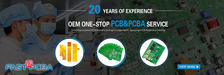
FASTPCBA is a professional PCB and PCBA manufacturer in Shenzhen, China. We provide high-quality bare PCB and PCB assembly services to global customers, including component sourcing, functional testing, conformal coating and full assembly.
FASTPCBA provides high-quality services for the global automotive electronics, medical electronics, telecommunications, industrial control, smart home and other industries.
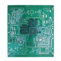
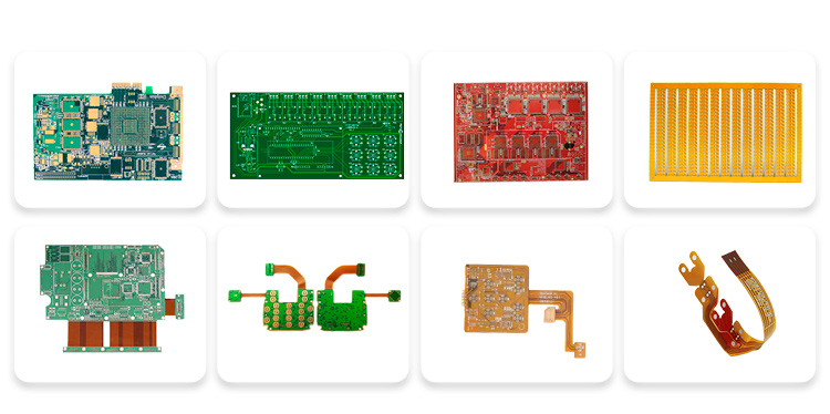
Bare PCB Manufacturing
Provide: rigid PCB; flexible PCB; rigid-flex PCB; high density circuit board; gold-plated PCB; high frequency PCB; aluminum substrate; copper substrate circuit board; high TG PCB; thick copper PCB…
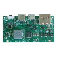
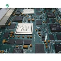
PCB Assembly Services
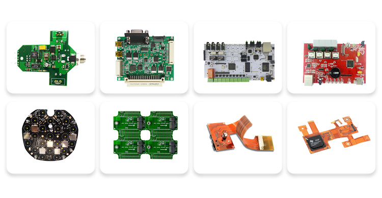
We have a global sales team to assist you with PCB manufacturing and PCB assembly services,Send your PCB files now for a better price!
| article | describe | ability |
| laminate | FR4, High TG FR4, High Frequency, Alum, FPC | |
| Sheet cutting | layers | 1-48 |
| Minimum thickness of inner layer (except copper thickness) |
0.003 in (0.07 mm) | |
| plate thickness | standard | (0.1-4mm±10%) |
| minute. | Single/Dual: 0.008±0.004” | |
| 4 layers: 0.01±0.008” | ||
| 8 layers: 0.01±0.008” | ||
| bow and twist | no more than 7/1000 | |
| copper weight | External copper weight | 0.5-4 0z |
| Inner copper weight | 0.5-3 0z | |
| drilling | smallest size | 0.0078” (0.2mm) |
| Drill deviation | ±0.002″(0.05mm) | |
| PTH hole tolerance | ±0.002″(0.005mm) | |
| NPTH hole tolerance | ±0.002″(0.005mm) | |
| Solder mask | color | Green, white, black, red, blue... |
| Minimum Solder Mask Gap | 0.003 in (0.07 mm) | |
| thickness | (0.012*0.017mm) | |
| silk screen | color | White, black, yellow, blue... |
| smallest size | 0.006 in (0.15 mm) | |
| Component Sourcing | Yes | |
| Tolerance of PCB | ±5% | |
| Maximum size of finished board | 700*460mm | |
| Minimum order quantity | No MOQ (1 piece) | |
| surface treatment | HASL, ENIG, Immersion Silver, Immersion Tin, OSP… | |
| Circuit board shape | Square, round, irregular (with clamp) | |
| pack | QFN,BGA,SSOP,PLCC,LGA | |
| Subassembly | plastic, metal, screen | |
| Minimum line/space | 0.075/0.075mm | |