Professional Engineer Rapid Schematic Electronic PCB Design and Software Development Fabrication PCB Layout Design
- $1.00 / 1 - 499 pieces
$0.50 / >=500 pieces - 1 piece
- ShenZhen ZhongYiLong Electronic Technology Co,. Ltd
- Guangdong, China
- Mr FengFu Li
PRODUCT DETAIL
| Supply Ability: | 99999 Pieces per Month; | Brand Name: | ZYL; |
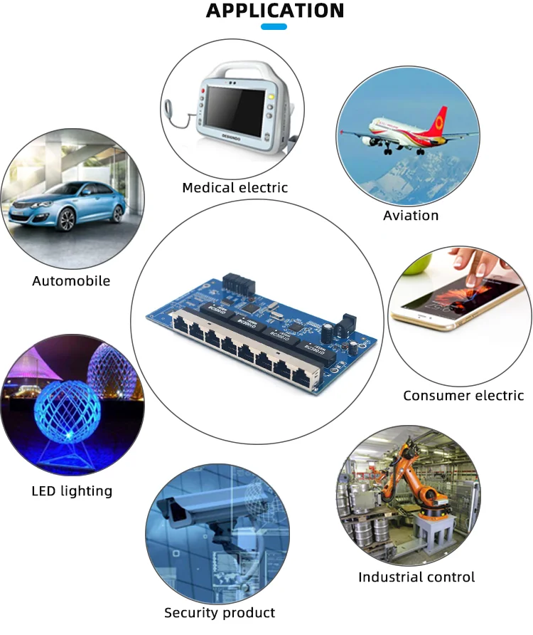
| Payment Terms: | L/C,T/T,Western Union,MoneyGram; | Application: | Electronics Device; |
| Material: | FR4 /aluminum/ceramicCEM1; | Number of Layers: | 1-20 Layers; |
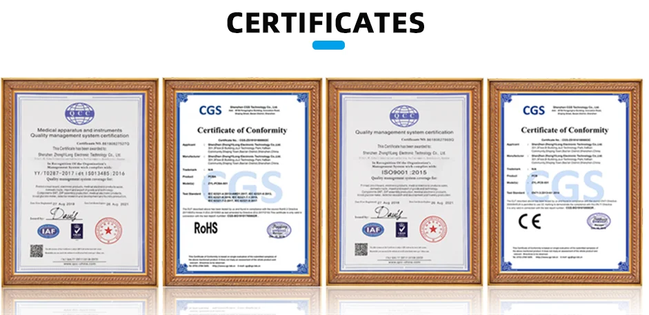
| Certificate: | CE ROHS; | Packaging Detail: | 1.Inner: PCB: Vacuum Packing PCBA: ESD Packing 2.Outer: Standard export carton; 3.Customized package.; |
| Solder mask color: | White.Black.Yellow.Green.Red.Blue; | Item: | ODM OEM design PCBA; |
| Port: | ShenZhen / HongKong; | Min. Line Width: | 4mil(0.1mm); |
| PCB Standard: | IPC-A-610 D/IPC-III Standard; | Board Thickness: | 1.6MM; |
| Model Number: | ZYL-PD-01A; | Surface Finishing: | HASL Lead free; |
| Solder mask: | Green. Red. Blue. White. Black.Yellow; | Product name: | Pcb Board design; |
| Min. Hole Size: | 0.20MM; | Min. Line Spacing: | 4mil(0.1mm); |
| Base Material: | FR-4; | MOQ: | 1pcs; |
| Copper Thickness: | 1OZ; |
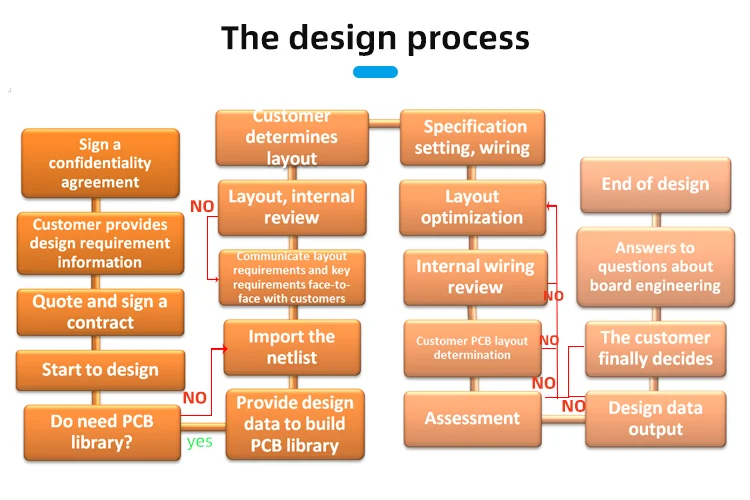
PCB Layout design
Design overview:
The company provides customers with efficient and high-quality services with professional PCB design concepts, excellent PCB
LAYOUT team, and strict design process; the company provides PCB impedance calculation and stack design for customers free of
charge; we support mainstream design tools in the industry: Allegro, Pads, Altium, etc., schematic tool support: CIS/ORCAD, Protel
DXP, Design Capture, etc.
LAYOUT team, and strict design process; the company provides PCB impedance calculation and stack design for customers free of
charge; we support mainstream design tools in the industry: Allegro, Pads, Altium, etc., schematic tool support: CIS/ORCAD, Protel
DXP, Design Capture, etc.
Materials to be provided for PCB design
1. schematic diagram :complete electric document format that can produce correct netlist;
2. mechanical size :provide the specific position and direction identification of positioning device ,as well as the
identification of specific height limit position area ;
3. device packaging :provide device packaging library or electronic material specification ;
4. wiring guide :description of specific requirements for special signals ,as well as design requirements for impedance
,lamination ,etc.
Design parameters
PCB max design layers | Unlimited | Max design PIN number | 60000 | Max number of design connections | 42000 |
Design min line width | 2.5mil | Design min spacing | 2.5mil | Design min aperture | 4mil;laser perforation |
Max number of BGA | 10 | Min BGA PIN spacing | 0.4mm | Max BGA PIN number | 4200 |
Max number of network | 15000 |
The design delivery
Single PIN number | 0-1000 | Design delivery (working days ) | 3-5 days | |||
2000-3000 | 5-8 days | |||||
4000-5000 | 8-12 days | |||||
6000-7000 | 12-15 days | |||||
8000-9000 | 15-18 days | |||||
10000-12000 | 18-20 days | |||||
13000-15000 | 20-22 days | |||||
15000-18000 | 22-25 days | |||||
18000-20000 | 25-30 days | |||||
Ultimate delivery capacity | 10000 PIN /7 days | |||||
Tips : the above delivery date is the convention delivery date .the accurate design evaluated according to the number of components degree of difficulty ,number of layers and other factors of the circuit boar . | ||||||
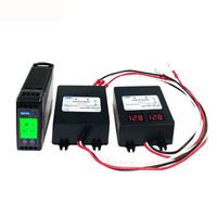
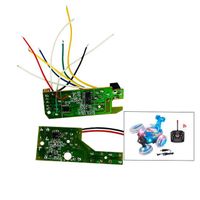
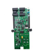
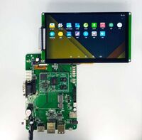
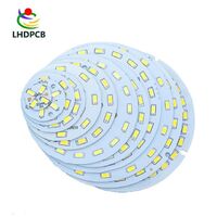
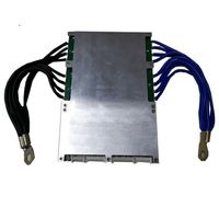
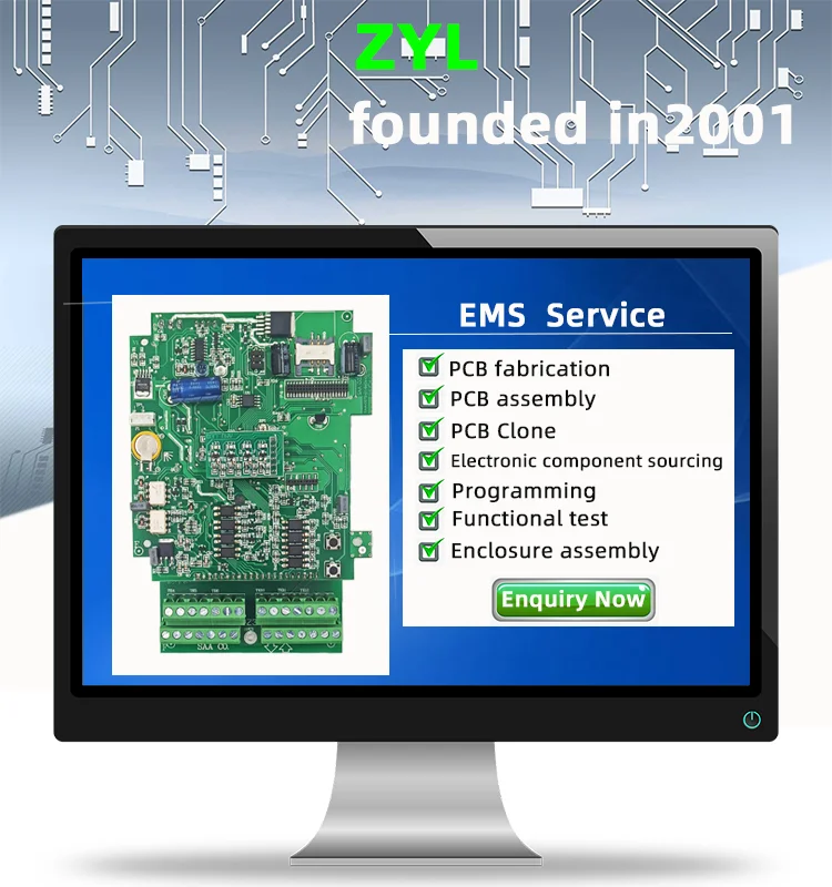
Involved in the product
Design Case Presentation
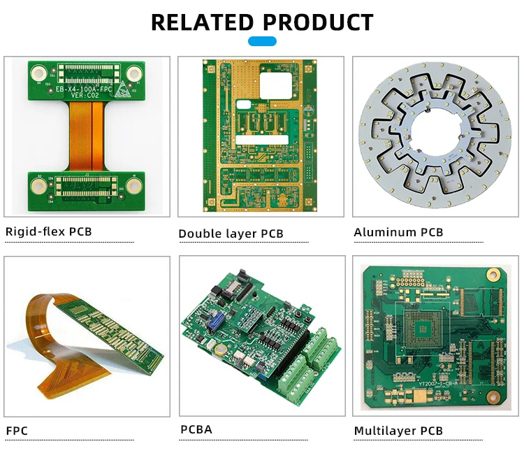
Related Product
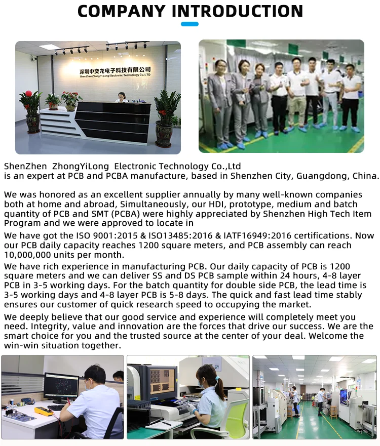
About us
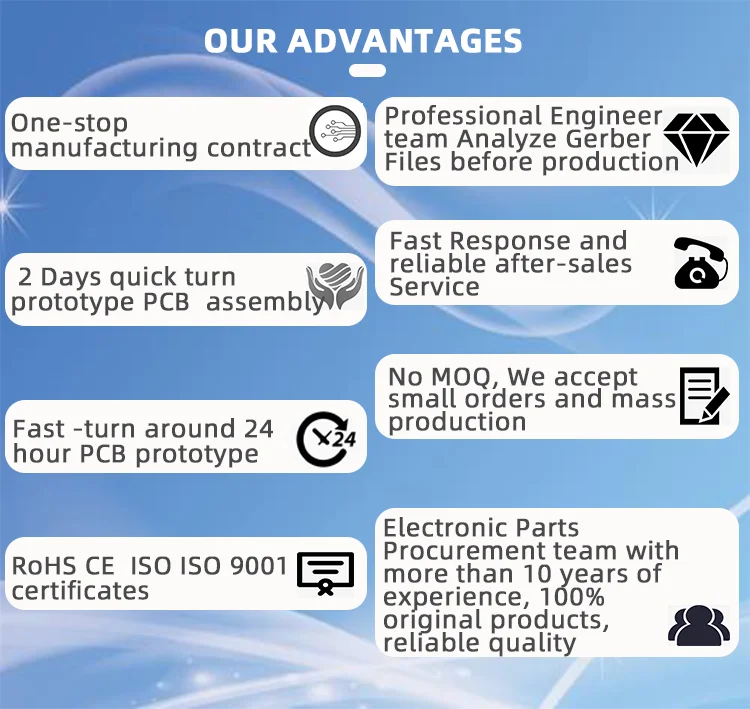
Our Advantages
Certifications
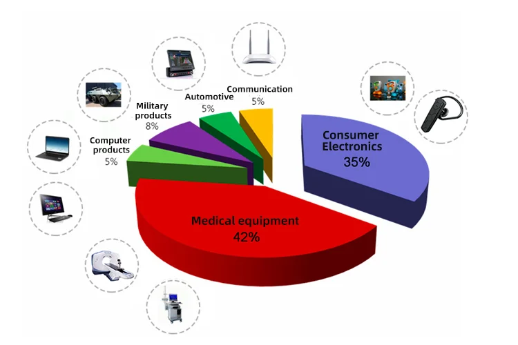
product application
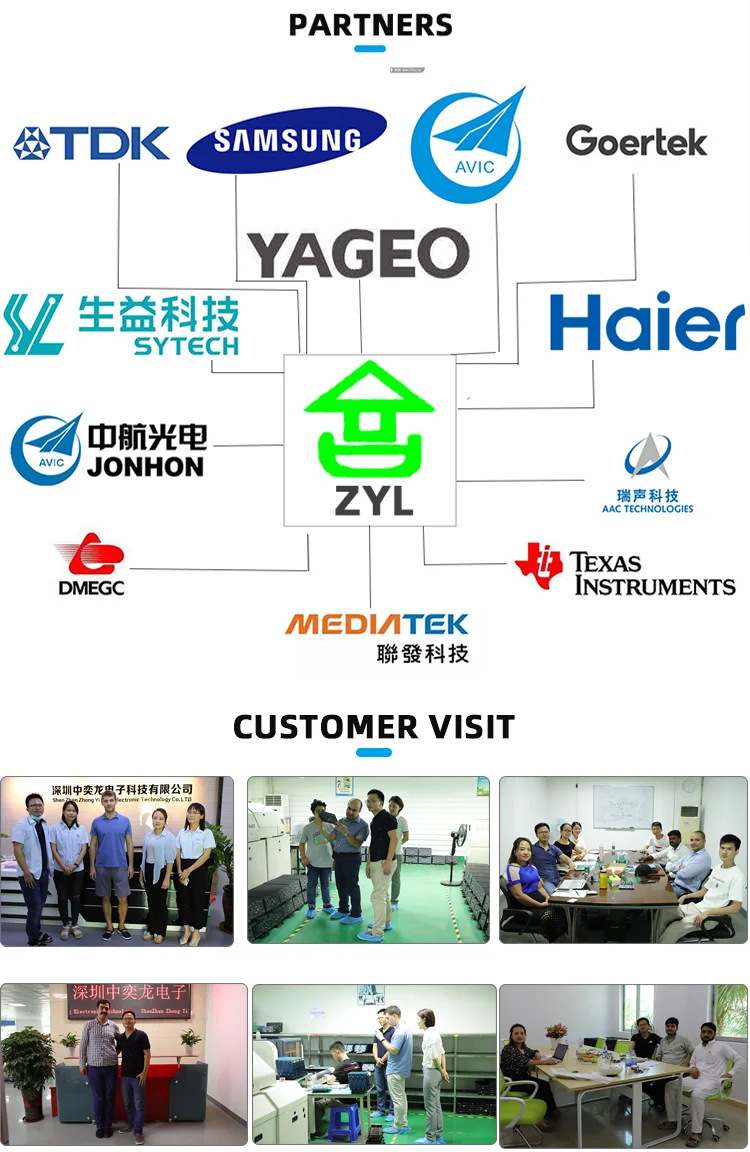
Partners

1. What professional service we offer ?
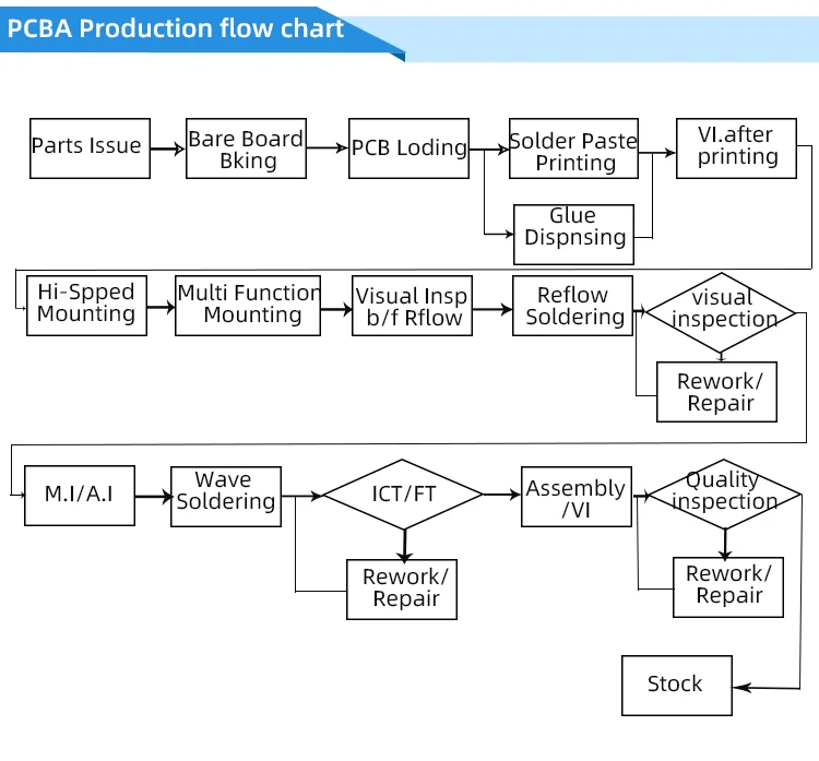
PCBA One-stop OEM service from PCB manufacture , Components sourcing , and then Assembly in house .
2. High quality control ability.
We provide 100% ICT Testing & 100% Function Testing for High quality control
3. MOQ.
No MOQ , and we provide samples testing before Mass production
4. Fast Delivery time.
PCB Samples or medium orders , 5-7 days, Mass production 2 weeks
PCBA samples or medium orders , 10-15days , Mass production 3 weeks.

VIEW MORE
YOU MAY LIKE